
Integrated Photonics Bootcamp at the LEAP (Lab for Education and Application Prototypes) Network in Massachusetts
A shortage of skilled engineers and technicians has impacted advanced manufacturing sectors in the U.S. over the past decade. Rapid skilling in STEM fields requires training on costly, maintenance-intensive, advanced manufacturing tools and innovative education programs matching the needs of employers.
A three-day integrated photonics bootcamp, held from Mar 22 to 24, was organized by the Initiative for Knowledge and Innovation in Manufacturing (IKIM), AIM Photonics, and Bridgewater State University and was led by Anuradha Agarwal, principal research scientist from the LEAP at IKIM, and Prof. Samuel Serna from the LEAP at Bridgewater State University.
Lecture topics focused on photonic devices, their applications, and application-specific photonic device packaging challenges. Bootcamp participants also performed hands-on experiments in integrated photonics packaging and testing, including:
Tool operations, with a die bonder, a reflow oven, and an x-ray imager
Edge and grating coupling of a fiber to the AIM Photonics education chip (The AIM Photonics education chip was designed by RIT’s Professor Stefan Preble, University of Rochester’s Professor Jaime Cardenas, and Boston University’s Professor Milos Popovic, under the leadership of MIT Professor Lionel Kimerling.)
Characterization of an optical parametric oscillator (laser), as well as a fully fiber-attached photonic chip
“We were fortunate to have Dr. Sebastian Skacel and his team from Vanguard Automation provide their photonic wire bonding demonstration, and Dr. Nicholas Fahrenkopf, photonics engineering manager at AIM Photonics, for his talk on the current and future capabilities of photonics foundries for the manufacturing of integrated photonic prototype devices,” Agarwal said.
“Enrollment in the bootcamp—which included college undergraduates, research university graduate students, and an incumbent company employee—was intentionally limited to 12 attendees to ensure sufficient tool-time for all participants,” said Samuel Serna, assistant professor of Physics, Photonics, and Optical Engineering at Bridgewater State University. After a two-year hiatus due to COVID-19, Serna noted that the bootcamp instructors and organizers were excited to return to a more interactive, in-person event with plenty of one-on-one time to teach in a blended environment with a strong hands-on component supported by lectures.
In addition to the lectures and hands-on learning activities, students also had the opportunity to experiment with virtual learning tools designed to help them more intuitively understand photonic device functionality, such as VM-Lab's Desktop Virtual Reality Device Simulations and a die bonder tool-simulation co-developed with Clemson University’s Center for Workforce Development.
“I’m incredibly proud of our integrated photonics bootcamp team for creating and offering this impactful hybrid learning experience, which uses three important pedagogical tools: lectures, simulations and hands-on lab work,” said IKIM Director Lionel Kimerling.
“Hands-on integrated photonics education and workforce development is a critical focus area at AIM Photonics,” said Robert Geer, director of Education and Workforce Development at AIM Photonics, “and we take pride in preparing the next generation to make breakthroughs in this nascent field.”
The bootcamp instructor team consisted of faculty, staff, and pre-trained graduate and undergraduate students from Massachusetts Institute of Technology, Bridgewater State University, and National University of Colombia. Agarwal noted that this approach turned out to be a highlight for student instructors, who reinforced their learning through teaching. “This is an innovative model showing promise, and we will continue to develop it in the future,” said Serna, whose undergraduate student trainer from Bridgewater State University, Samuel Bechtold, mentioned that “An added benefit is that it provides an opportunity for photonics community building and networking.”
Jadyn Lee, an undergraduate student at Stonehill College, Massachusetts, said, "This was an amazing opportunity and helped me realize I have made the right career choice. I'm excited to see where photonics takes me in the future.”
“We're equally excited to inspire the imaginations of young students and help direct their professional course towards rewarding STEM careers, through such an innovative hybrid-training program,” said Dr. Sajan Saini, Education Director at IKIM.
This second AIM Photonics bootcamp offered in Massachusetts, was delivered through a partnership between the LEAPs at MIT and Bridgewater State, which are two in a network of five LEAPS within Massachusetts. The next AIM Photonics bootcamp offered in partnership with the LEAPs is planned in January 2023.
Drew Weninger, graduate student at the Department of Materials Science and Engineering at MIT, teaching Peyton Brown (seated), undergraduate student in Physics at Bridgewater State University, about ensuring alignment prior to picking and placing a die onto a substrate, during a hands-on experiment in die bonding at the MRSI M3 die bonder in the LEAP at MIT.nano.

Luigi Ranno, a graduate student at the Department of Materials Science and Engineering at MIT, demonstrates testing of packaged LEDs, in the LEAP at MIT.nano. The LEDs in the die bonded package light up to show the letters “PIC” for Photonic Integrated Circuits, when powered, demonstrating successful die bonding.

Kenan Cicek, a Fulbright Scholar at IKIM, MIT, teaches (L to R) Gillian Micale, a graduate student in the Department of Materials Science and Engineering at MIT, Yasaman Sargol, an engineer at Seurat Technologies, and Samuel Bechtold, an undergraduate student in Physics at Bridgewater State University, how to use the PXI GenX-130 X-ray imager and how to evaluate the die bonds on their package to ensure that there are no voids after completion of the pick and place and solder reflow processes.

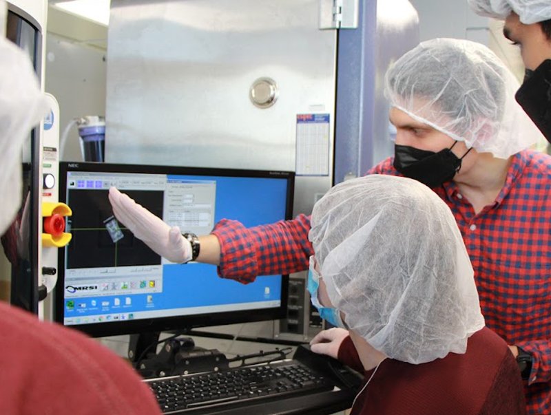
Prof. Samuel Serna, Assistant Professor of Physics, Photonics, and Optical Engineering at Bridgewater State University, explains how to gather data from a ring resonator on the AIM Photonics Education chip. Sharp resonant peaks of the ring resonator are visible on the screen as he is in the process of aligning a fiber to the edge of the chip, using a Maple Leaf probe station in the LEAP at Bridgewater State University.

Lectures for knowledge dissemination. Shown at top, is Dr. Sajan Saini, Education Director at IKIM discussing applications of photonic integrated circuits, and, at bottom, Juejun Hu, Associate Professor, Department of Materials Science and Engineering at MIT, teaching how multi-mode interferometers can be used to manipulate light on-chip.